English
 English
 Deutsch
 Español
 عربي
عربي हिंदी
हिंदी

Brand:HOMNECKS
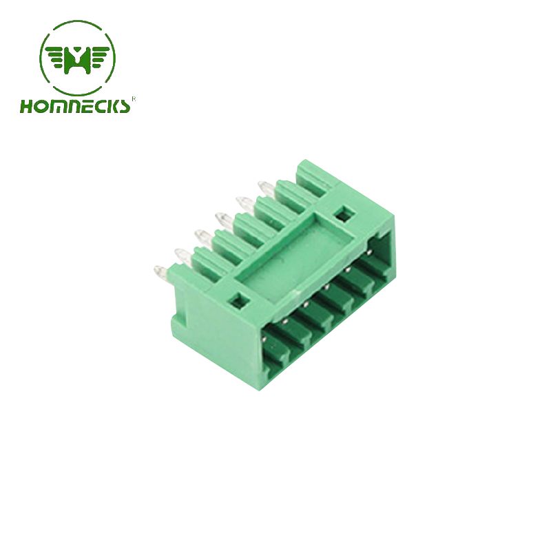
2.54mm (equivalent to 0.1 inch) is a very classic and universal spacing standard in the electronics industry, originating from the pin spacing of imperial integrated circuits. The straight pin design is the most basic and commonly used form of such terminals.
Item No :
H2EDGCV-2.54Payment :
T/TProduct Origin :
ChinaColor :
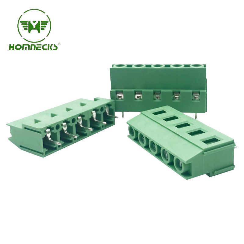
green ,we can also make other color if meet moq2.54mm PCB Pluggable Terminal Block Male Header
As the name suggests, a straight pin refers to the pin part connected to the PCB board that is straight and perpendicular to the terminal body and the PCB board plane..
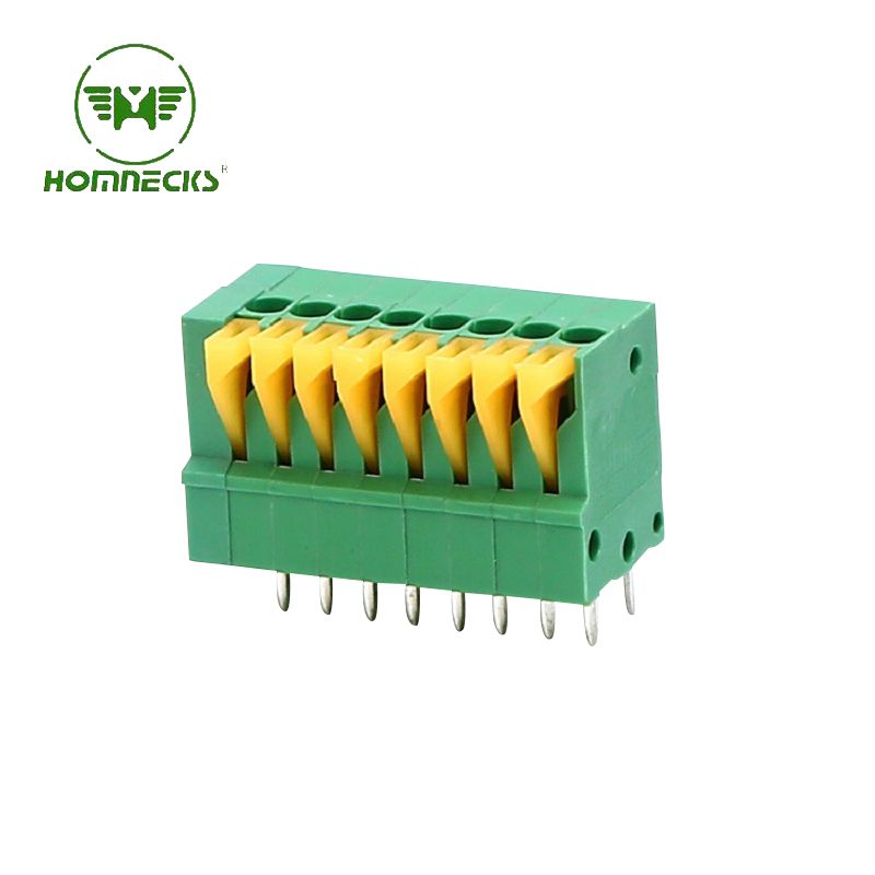
1.Type and Pole
Type: Pcb Pluggable Screw Terminal Block
Pole:
| 2 pin terminal block | 3 pin terminal block | 4 pin terminal block | 5 pin terminal block | 6 pin terminal block | 7 pin terminal block |
| 8 pin terminal block | 9 pin terminal block | 10 pin terminal block | 11 pin terminal block | 12 pin terminal block | 13 pin terminal block |
| 14 pin terminal block | 15 pin terminal block | 16 pin terminal block | 17 pin terminal block | 18 pin terminal block | 19 pin terminal block |
| 20 pin terminal block | 21 pin terminal block | 22 pin terminal block | 23 pin terminal block | 24 pin terminal block |
1. Design structure and material
Shape: Typically cylindrical or square pins protruding vertically from the bottom of the terminal insulation body.
Material: Formed integrally with the terminal conductor, typically:
Brass: good strength and conductivity, high cost-effectiveness.
Electroplating: To enhance solderability, prevent oxidation, and improve corrosion resistance, the surface of straight pins is typically subjected to electroplating treatment.
Tin plating: the most common choice, low cost, good solderability.
2. Mechanical structural characteristics
Crimp/rivet fixation: A straight pin does not simply insert into the plastic body of the terminal. Its tip usually features a barb, knurling, or riveting structure. During the injection molding or assembly of the terminal, the plastic fills or wraps around this structure, forming an extremely strong mechanical connection that prevents the pin from being pulled out of the body.
Coplanarity: For multi-position terminal blocks, the bottoms of all straight pins must lie on the same absolute plane. This characteristic is known as coplanarity. High coplanarity ensures that all pins can make good contact with PCB pads simultaneously, which is key to achieving high-quality soldering
2.Material Of Pluggable Terminal Block
| Housing | PA66, UL94V-0 |
| Pin header | Copper alloy ,Tin Plated |
This is the core area where the straight pin terminal forms electrical and mechanical connections with the circuit board.
1. Coordination between pins and pads
PCB pad: PCBs are designed with through-hole pads that correspond one-to-one with terminal pins. The diameter of the through-hole is slightly larger than the pin diameter to allow space for the solder to climb through capillary action.
Matching of pin diameter and through-hole diameter: This is a key design consideration. The through-hole diameter is usually 0.2-0.4mm larger than the pin diameter. For example, a pin with a diameter of 0.64mm will be matched with a PCB through-hole with a diameter of approximately 0.9-1.0mm.
2. Welding process
Straight pin terminals are mainly soldered using through-hole technology.
Wave soldering:
Plugin: Insert the straight pin of the terminal into the corresponding through hole on the PCB.
Fluxing: The bottom of the PCB passes through a flux spray zone to remove oxides and enhance solderability.
Preheating: The PCB enters the preheating zone to prevent thermal shock when it comes into contact with molten solder.
Soldering: The bottom surface of the PCB is subjected to a "wave" of molten solder raised by a pump. The solder is drawn into the through-hole by capillary action, forming a complete solder joint filling between the lead and the pad.
Cooling: Form a firm electrical and mechanical connection.
Manual soldering:
Suitable for small-batch production, repair, or replacement. Use a soldering iron and solder wire to solder each solder joint individually.
3. Solder joint morphology and requirements
A high-quality solder joint should possess the following characteristics:
Full filling: The solder should fill 100% of the through-hole and form a small conical meniscus on the bottom surface of the PCB.
Good contact angle: The contact angle between the solder and the lead and pad should be smooth and rounded, indicating good wetting.
Bright and smooth: The surface of the solder joint should be bright, free of burrs, and without pores.
3.Electrical Of Pluggable Terminal Block
| Rated Voltage |
UL IEC 150V 130V |
| Rated Current | 5A 10A |
| Contact Resistance | 20mΩ(MAX) |
| Insulation Resistance | 500MΩ/DC500V |
| Withstanding Voltage | AC 1250V/1 Min |
4.Mechanical Of Pluggable Terminal Block
| Temp. Range | -40℃~ +105℃ |
| MAX Soldering | +250, for 5 Sec. |
5.Dimensions

6.Advantages
☑ Adapt to multi-type sockets, device design is highly flexible
☑ Keying requirements can be met
☑ Universal installation method, suitable for various situations
Advantage:
Extremely high mechanical strength: Through-hole soldering provides significantly higher mechanical strength than surface mount technology (SMT). The terminals themselves can withstand greater insertion and extraction forces as well as lateral stress from wires, making them less likely to detach from the PCB.
Reliable connection: The solder forms an all-round connection within the through-hole, with a large contact area, providing a very stable electrical connection and strong resistance to current impact.
Easy to detect and repair: The solder joints are visible to the naked eye, facilitating quality inspection. Tools such as tin suction devices can be used to disassemble and replace them relatively easily.
Cost-effectiveness: Through-hole technology is mature, with a simple production process, and still offers cost advantages in high-volume applications.
Design and application considerations:
Occupied PCB space: Through-holes require the entire thickness of the PCB board, and solder pads occupy space for bottom-layer wiring, making them less space-efficient than SMT devices.
Cannot be used for high-density assembly: In very compact modern electronic devices, the 2.54mm pitch itself is considered relatively large, and the THT process limits the wiring density.
Welding stress: During the wave soldering process, high temperatures may cause thermal stress on the plastic body of the terminals. It is crucial to choose high-temperature resistant materials, such as UL94 V-0 grade PA66.
Pin coplanarity: As mentioned earlier, poor coplanarity can lead to soldering defects or open circuits, making it a critical quality control point in production.
7.Application Of Pluggable Terminal Block
1.Motion controller 2.Three-phase power meter 3.Microcomputer protection device 4.Electric equipment
5.Automation equipment 6.Security equipment 7.Internet of things equipment
8.Package Of Pluggable Terminal Block
We choose the high quality and safe packaging material to make sure your order won't be damaged during delivery.
These trade terms are acceptable:EXW,FOB,CFR,CIF.

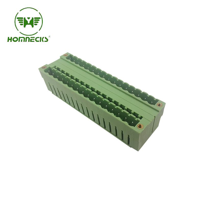
Brand:HOMNECKS Crafted with utmost precision and adhering to the highest industry standards, our 5.08mm Pitch Dual Row Straight Needle Terminal boasts exceptional reliability and durability. This makes it a perfect choice for your diverse range of electronic applications.
Details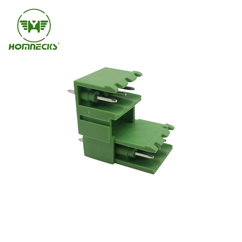
Brand:HOMNECKS 5.08 Dual Row Pluggable Straight Needle Terminal revolutionizes the way you operate in the world of electrical engineering.
Details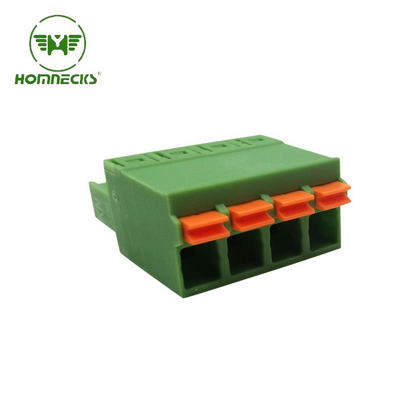
Brand:HOMNECKS Head for Pluggable Terminal Block , 5.08 Pitch,Screwless Numble Of Pole: we can make from 2P to 24P
Details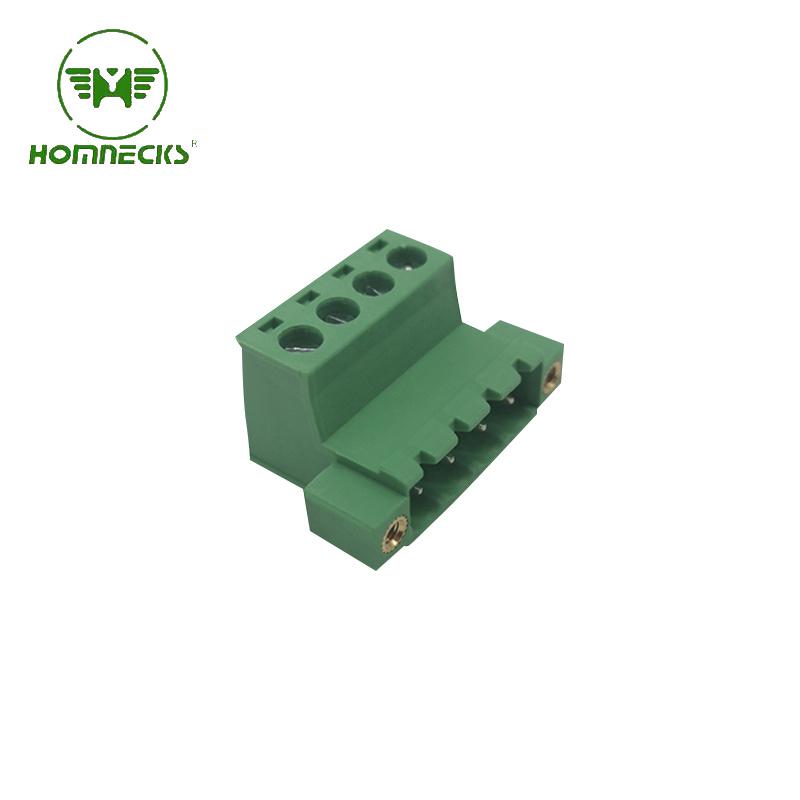
Brand:HOMNECKS 5.08 Pitch Pluggable Terminal Block Numble Of Pole: we can make from 2P to 24P
Details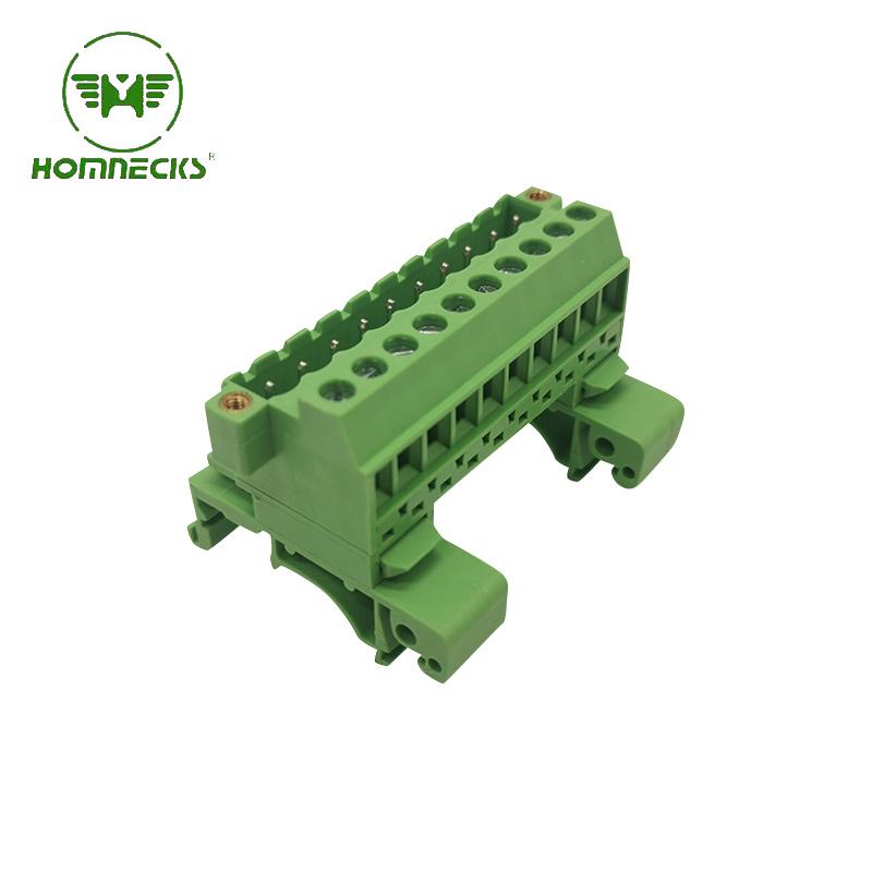
Brand:HOMNECKS Rail Plug-in type terminal block H2EUDBM-5.08
Details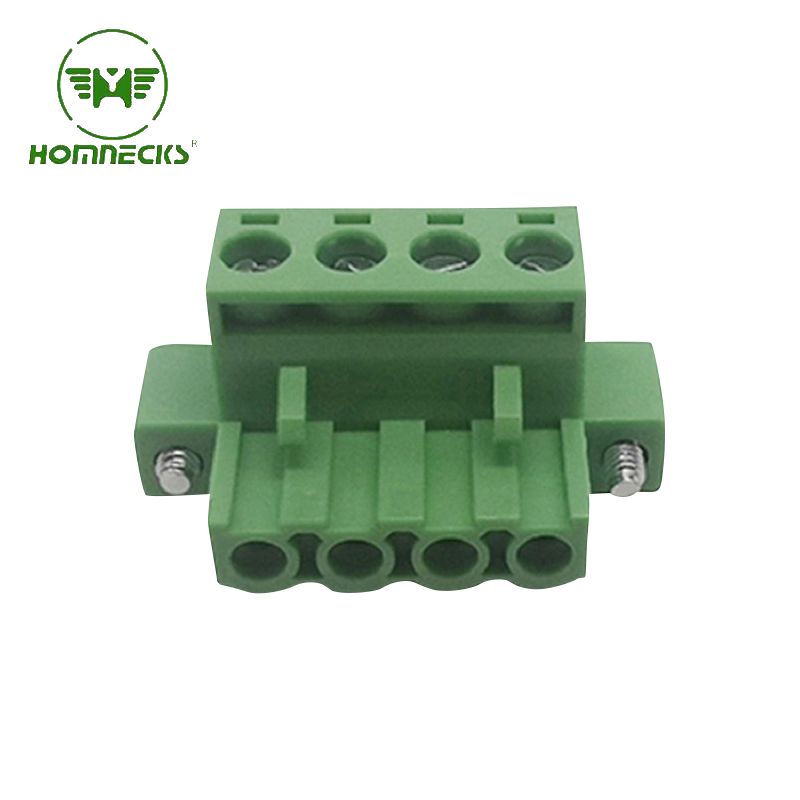
Brand:HOMNECKS Crafted with utmost precision, the housing is constructed from flame-retardant PA66 material, guaranteeing superior fire resistance. Complementing this, the metal components are expertly manufactured using copper plated with nickel, endowing the terminal with exceptional electrical conductivity.
Details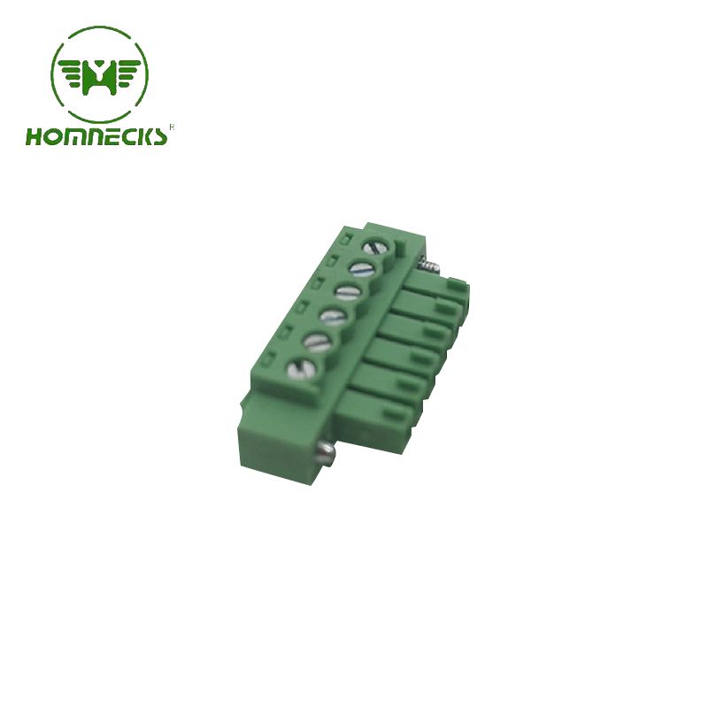
Brand:HOMNECKS Embrace professionalism and technical prowess with this phenomenal 3.81mm pitch PCB terminal. Take advantage of its remarkable features and unleash the full potential of your electronic endeavors. Experience excellence. Experience reliability. Experience progress.
Details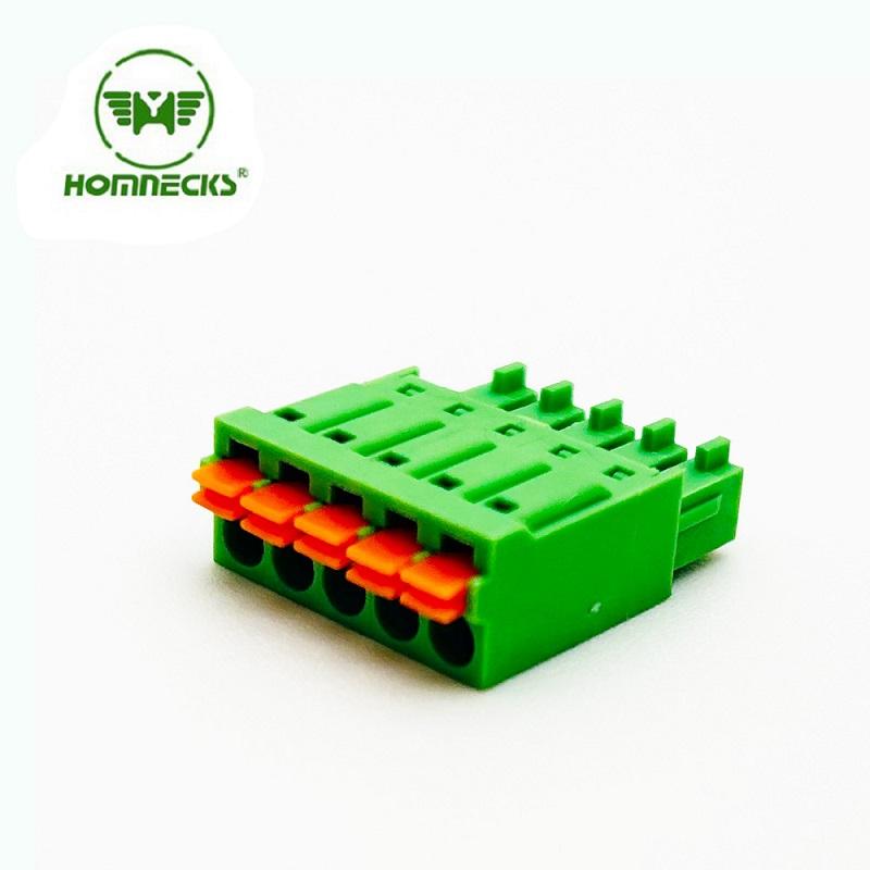
Brand:HOMNECKS 3.5mm pitch screw-less terminal connectors! Designed to optimize efficiency in your electrical projects
Details Contact Us
Signup our newsletter to get update information, promotion and insight.


 IPv6 network supported